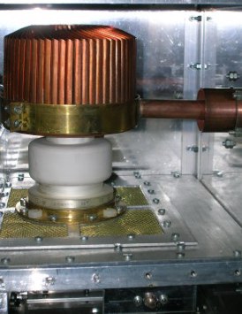
GS35b 144MHz cavity
This 144MHz power amplifier is based on the ideas, schematics and mechanical drawings earlier presented by DG2KBC. To understand the design, it is good to be aquainted with the electrical schematics that is on the internet.
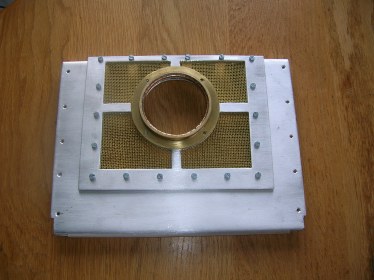
 Mechanical setup: Mechanical setup:This is a description how the cavity design, of which I found the mechanical drawings from DJ5RE on the internet, is done in my situation. The used material is aluminum, 3mm wall thickness and 10x10mm aluminum profile to join the edges. The 10x10mm aluminum profile is drilled and special nuts are press-fitted into the holes to give thread for the bolds. These press-fit nuts are needed because of the too thin wall-thickness of the aluminium profile (1,5mm). The special nuts to ensure enough thread.
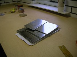
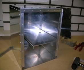 The picture above shows the pile of aluminum plates, cut to the dimensions DJ5RE shows. After a couple of evenings, the results is a square box. In the picture to the right, one can already recognise the podest on were in a later stage the homemade tube-socket will be mounted.
This amplifier uses a quarter-wave resonator that is mounted next to the tube. The resonator is made from a plate of brass, connected to ground at the bottom of the cavity-box.
Coupling capacitor:
The top of this resonator is connected by means of a big disc capacitor to the anode of the GS35b. Do not use a too small disc capacitor that is not rated the expected RF-current in combination to the RF and DC-voltages during operation. My firsts tries ended ina big bang, were the 1000pF/4kV disc capacitor got punched at two places. Two places one can ask....? Indeed two times because after the first flash-over, no low-ohmic path in the cavity could be found and all looked fine. Also the tube was not suspected and thus I decided to re-connect everything and tried again. As soon as the DC-plate voltage was applied, again all fuses went up in smoke and there I found the two black markings on the disc capacitor...
Advice is to use a 470pF capacitor, russian making and showing a kVar value of no less than 40kVar. DC voltage of this large disc capacitor was 15kV. A good lesson in materials, because some more study afterwards indeed shows different capacitors on the market, meant for different usage. Capacitors without any kVar marking should never be used in this situation as these are not meant for RF signals!
  In the above two pictures, the used disc capacitors are shown. On the left is the punched, 1000pF/4kV small disc capacitor, on the right picture the two larger ones are of better choice. I now use the 470pF, 15kV/40kVar type and this gives a stable setup and the rated output power. For purchasing these capacitors I advice to take a look at the web-pages of dr. Alex Gavva, www.nd2x.net/ur4ll.html Compare in this picture the size difference between the no-go 1nF/4kV type and the 470pF larger one.
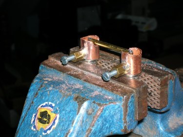
Plate-capacitor (PA0JCA-style):
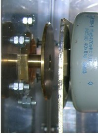
When lookin at the DJ5RE mechanical drawing, the plate-tuning was done by moving a conductive plate towards the anode of the tube. During a HAM-meeting I came across Sjaak, PA0ACJ, and he gave me a nice idea to make the tuning more reliable. The construction Sjaak uses, can be made from regular plumbing materials. The idea is to create a plate capacitor from two copper-tubes that slide into each other. There is a large difference in diamter chosen to avoid flash-over. The outer-tube is adjustable, the inner-tube is silver-soldered to the clamping ring that is running around the GS35b's anode. This small copper tube has 12mm outer diamter and is positioned exactly opposite the connection of the prior decribed disc capacitor. Take care of some isolation in between the two tubings. I have some bad experience in which a signle sheet of PTFE (teflon) was insufficient to the voltages that occur. In the picture here you can see the results what happens then. Unfortunate the internet is not a good medium to also give the belonging sound that comes from such a not-planned firework hihi...
 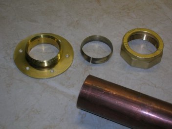 When copyin this method of plate-tuning, don't forget to make a small cut by means of a iron-saw in the ring that normally secures the tube in place. The nice trick from Sjaak is that the cut in the ring gives the possibility to tighten the big brass nut and when needed, it can be loosen again, releasing the small ring a bit. When tuning is ready, the outer tube can be fixated again t\in the new position and giving good RF-contact again to the outside wall of the cavity.
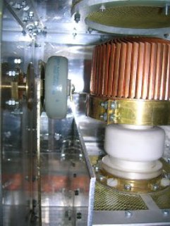 Position of anode-clamp Position of anode-clampWhen looking at the picture were the assembly is shown for the plate
capacitor, pay attention to were the ring around the anode of the GS35b is situated. This is not the location that is shown in the DJ5RE design! However the height of the output line is exactly the same as DJ5RE is giving. This is done to get a nicer method of connecting the disc capacitor. These have two screw terminals at both sides and a small piece of brass gives just the space need to reach this screw at the anode-side of the GS35b. In the picture to the right this is show:
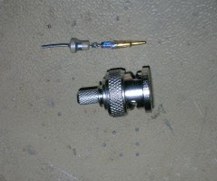
Tube socket:
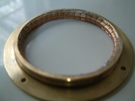
The tube socket is home made. It is made from a piece of 2mm brass plate that is cut and
 filed to round shape. The grid contact ring is soldered on top of this brass plate and fingerstock material is soldered into the ring. It was quite hard to find exactly a piece of brass tuning that together with some spring force of the fingerstock material had the right inner diameter. At the time of the build I had no lathe available to machine a ring from a little too less inner diamter material. Therefore I deciced to a piece of brass tubing that had the next larger inner diameter compared to was needed. I made a ring of 7mm height and cut a piece of material from it. I then pressed the ring while checking the inner-diameter with fingerstock on right spring force. After two or three more material cuts (every time 1 or 2 mm...) the outer diamter could be measured. This was now cut from the 2mm brass plate that is meant to be screwed on top of the aluminum plate that holds the tube socket in the cavity. The brass ring is now (while pressed togehter) soldered into the opening. This method is chosen to have more soldering area and give more strenght. Also because of the ring now pressed into the opening of the brass plate material, the soldering of fingerstock material into the grid ring is made very easy. The ring cannot widen itself any more because of the tight fitting into the plate. filed to round shape. The grid contact ring is soldered on top of this brass plate and fingerstock material is soldered into the ring. It was quite hard to find exactly a piece of brass tuning that together with some spring force of the fingerstock material had the right inner diameter. At the time of the build I had no lathe available to machine a ring from a little too less inner diamter material. Therefore I deciced to a piece of brass tubing that had the next larger inner diameter compared to was needed. I made a ring of 7mm height and cut a piece of material from it. I then pressed the ring while checking the inner-diameter with fingerstock on right spring force. After two or three more material cuts (every time 1 or 2 mm...) the outer diamter could be measured. This was now cut from the 2mm brass plate that is meant to be screwed on top of the aluminum plate that holds the tube socket in the cavity. The brass ring is now (while pressed togehter) soldered into the opening. This method is chosen to have more soldering area and give more strenght. Also because of the ring now pressed into the opening of the brass plate material, the soldering of fingerstock material into the grid ring is made very easy. The ring cannot widen itself any more because of the tight fitting into the plate.Of coarse everything would be much easier in case someone can machine such a assembly on a lathe, but I want to share my method here and show that also by using a iron-blade saw, a file and some patience, the result is also perfect...
The rest of the tube socket is not very difficult to make. Two pieces of 1mm brass plate are cut into a square shape. Into the two plates holes are made in such diameter that together with the fingerstock material good contact is achieved to the tube.
Important: Drill prior to insertion of the fingerstock material 4 holes through the total assembly of the tube socket. These 4 holes must align insuch a way that 4 nylon bolts can be used to create the correct distances.
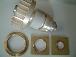
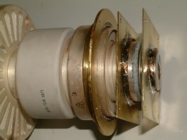
Below are three detailed pictures showing how it should look like:
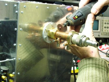
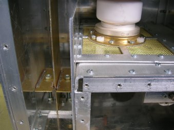
   Chimney contruction
At the time this picture was taken. there was no chimney mounted yet at the top of the anode. This was not needed at first tests, however after also tests were performed in FSK441 and JT65b, the inetrior of the cavity was warmed lightly due to some irregular airflow. It was decided to build a PTFE (teflon) chimney on top of the tube to be sure that the warm air was let directly to the outside of the cavity. the chimney is made from some sheet material, rolled exactly to the tube's anode diameter. Strips of thin copper-tape were soldered at both ends of this PTFE tube and soldered. The hole on top of
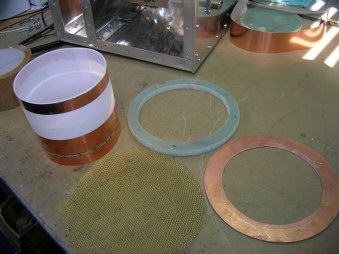 the cavity is large enough to be able to feed the tube in the tube-socket from the top. After the tube is fitted in place, the PTFE tube chimney is lowered over the anode, pressing it down until the bottom of the chimney touches the ring were the plate-capacitor as well as the coupling disc capacitor is mounted to. Now the chimney is made to such length that is rages out the cavity at the top for a few milimeters. A round piece of brass mesh is now placed over the chimney and a 6mm thick glas-fibre ring is screwed to the top of the cavity. This method secures the tube in place in the socket. That is very important, because during transport there must be no force to the coupling disc capacitor, nor movement in the plate-capacitor. the cavity is large enough to be able to feed the tube in the tube-socket from the top. After the tube is fitted in place, the PTFE tube chimney is lowered over the anode, pressing it down until the bottom of the chimney touches the ring were the plate-capacitor as well as the coupling disc capacitor is mounted to. Now the chimney is made to such length that is rages out the cavity at the top for a few milimeters. A round piece of brass mesh is now placed over the chimney and a 6mm thick glas-fibre ring is screwed to the top of the cavity. This method secures the tube in place in the socket. That is very important, because during transport there must be no force to the coupling disc capacitor, nor movement in the plate-capacitor.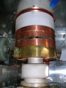 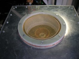 The second ring in the picture, showing the seperate parts of this chimney, is made from double clatch FR4, 1.5mm thickness. This ring is soldered around the upper copper band around the PTFE chimney and covered around the edges with sticky copper-tape. After inserting the chimney down into the cavity, this double-clatch FR4 board is just touching the top of the cavity. Together with the brass mesh this ensured good RF shielding once the 6mm ring is screwed in place. The brass mesh is very thin and ensures no resistance for the airflow. This mesh is also used in the socket area for the same reason.
 Output line
From the electrical schematics can be seen that the output of the amplifier is capacitive coupled to the resonator line (CL). This capacitor is made from a 50mm diameter brass disc. Again the proven contruction (thanks to Sjaak, PA0JCA) of the plate capacitor is used to move the output line closer or further away to or from the resonator line.
In the picture to the right, the output coupling disc is shown. Here is already the bigger RF-coupling disc capacitor disc from anode to resonator shown. This one proved to be able to withstand the high voltages and currents during some extended high power tests...
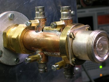 Directional coupler:
A view on the outside of the cavity,to the output line, shows some additional functionallity compared to the original design. Here is a directional coupler mounted to measure both forward and reflected power. This directional coupler gives a DC-voltage that is direct related to the measured power. The DC-voltage is generated by means of two small signal diodes BAT42, one for forward and the other to measure reflected power. The coupling lines are terminated by means of small resistive loads, build inside a BNC-plug like also the rectifying diodes are placed inside BNC plugs. The diode's are decoupled by feedthrough capacitors that exactly fit in the shaft of the BNC crimp-style BNC plugs. To prevent the forward diode to be in saturation, the coupling factor is chosen to be only -40dB. This is 20dB less compared to the reflected port. This reflected port is known to give normally very little voltage because of good VSWR and low amount of reflected power.
The four BNC chassis parts are fixed in place in small pieces of regular copper plumbing tube. To prevent them from melting (low cost plastic types were only available...), there are M3 bolts to the side. The inner pins of the BNC chassis-parts are interconnected by a small piece of brass staff material. Despite the short length of the coupling line, the position relative to the output centre line was this large that the coupling lines could not be kept within the outer diamter of the output line. That is why the coupling lines are after mounting was ready, were covered by small pieces of brass tubing cut along the long side of the 8x6mm tube.
Below are some pictures showing detail construction work on the directional coupler:
 Preparing one of the coupling lines. This complete assembly is soldered in one step to the outer tube of the output line. This turned out to be a delicate task because the soldering of the small 6-sided brass thread that holds the M3 bolds get loose easily. To prevent this from hapening, I wrapped a piece of stripped wire tightly around it while soldering the rest. After three tries, I succeeded finally. There are may be better and easier ways, but I have limited tools available...
 Here I m in the process of making the opening in the outer tube of the output line by means of a Dremel-tool. At this stage the first coupling line was already in place. The coupling factor was determined by connecting a RF-source at 144MHz to the output connetor of the cavity. Having the coupling-line terminated by a 50Ohm load, the coupling can be masured on the remaining BNC chassis part. The coupling lines were adjusted this long that the -40dB forward and -20dB reflected factor was reached. Very accurate this is not needed because the DC voltage from the diodes are in a later stage calibrated to show the right amount of forward and refelected power.
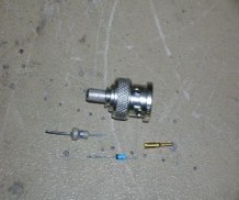 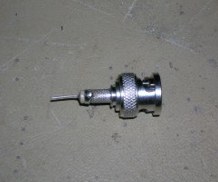  The three pictures above show how exactly the two diode detectors are build into the BNC crimp-style connectors. The feedthrough capacitors have 1nF and serve two goals: they smooth the rectified RF-voltage and at the same time they nicely centre the diode in the tube of the BNC plug.
Results:
After finishing the power supply unit (descibed on another part of the weg-site), it was time
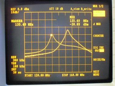 to check the functionallity. To have a good idea on the initial performance, a Spectrum-Analyser with tracking function was connected to the input and output of the completed cavity. to check the functionallity. To have a good idea on the initial performance, a Spectrum-Analyser with tracking function was connected to the input and output of the completed cavity. It now turned out that the resonance frequency of this cavity could not be tuned into the 144MHz band. The highest achievable frequency was only 135Mhz. hat could be wrong? All dimensions were exactly compared to the original drawing! Searching the internet on other users of this cavity gave indeed an answer: The resonator was too long...Some builders took huge measures to solve the problem by cutting the cavity by some 30mm in height! I did myself some tests and found that instead of using the GS35b using the slightly lower rated GS31b, gave good tuning. The picture of the tracking generator shows the trace of using both tubes for the test. The GS31b uses a smaller cooler and that explaines the behaviour for the low resonance frequency. The stray-capacitance of the GS35b bigger cooler de-tunes the resonance frequency a lot.
I did some tests on output power were the resonator was not cut to a shorter lenght but
 instead of this (unreversable) method, I made some sliderblocks from brass and fingerstock material. These 2 blocks were adjusted in such a way, that the resonance frequency was at 144MHz (plate capacitor in middle position). instead of this (unreversable) method, I made some sliderblocks from brass and fingerstock material. These 2 blocks were adjusted in such a way, that the resonance frequency was at 144MHz (plate capacitor in middle position). This immediate gave the desired result. In the picture on the left , this intermediate solution shown. The solution was usable, but still i was looking for a better way. Instead of shortening the resotor by some 30mm, I decided to increase its width! The formula's for resonance lines indicated that this increases the frequency in the same way as shortening the length. Now I increased the width of the resonator by a factor 2 compared to the original design and am able to still use the grounding position at the bottom of the cavity.
Output power achieved at 3kV plate voltage well exceeds the 1kW my SWR/POWER meter can indicate. Luckily I have now access to the DC-voltages from the diode detectors and started to build a new Power Supply Unit that uses this detecor voltages for indication at the front panel. With this also protection can be done for too high VSWR. Take a look at the other pages on this site to find out more on this nice PSU!
To complete the desciption, here is the drawing made by DJ5RE:
|