GS35b Power-supply (3.2kV / 3kVA)
This page descibes the build of my Power Supply Units that are in service for my 144MHz and 432MHz
GS35b amplifiers. I have first build one and soon after that a second one.
The PSU's are build after some study of other designs. From there several idea's have been re-used and also new electronics was designed to give a result that exactly matches the need.
Normally Power Supply Units build by HAM's uses analogue metering for plate current, anode voltage, grid current and so on, my idea was to have a modern way of presenting these value's. Looking at the nice project like HAM's build using materials delivered by others, I decided to use also LED bargraph inicators for all relative signals.
In my two GS35b PSU's, I now use LED metering for:
The PCB that holds the componets are own designed using EAGLE software. The PCB that gives the output towards the LED-indicators is a own design. That was needed because existing designs were not found that matches the intermediate signals. Triode control boards made by G3SEK are in use among many HAM's nowadays. However this design did also not give me the needed signals to control the LED board.
The controlboard features beside the signal conditioning for the LED bargraph's also the different protection circuits and delay timers. Below is a list that summeries the features of this controlboard:
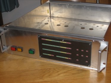
To have an idea how the PSU's look like, you may take a look at the picture below:
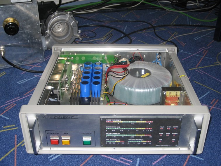 The PSU's are build around the heavy duty HV-4 toroid transformer delivered by a German firm called Eurofrequence Dierking. This firm also deliveres the capacitor bank that matches the transformer, but to save some costs, I decided to make that myself.
Below you can download files that you might need if you decide to build this PSU yourself. The drawings appear quite large on the screen, best is to right-click and use the function 'save picture'. Now you can use an external program to have a look at the drawings and use ZOOM IN/OUT to have a more convenient look. If you decide to use the LED-board, it is best to also use the logicboard (rev.B). This because the interfacing of the LED-board is designed for this. Remember that for instance measuring Anode-current in the tube is done floating, wich means dedicated design was needed to meet that requirement. To supply the logicboard and the LED-display, a separerate power-supply is needed, giving +5V and a second +5V but floating from GND. This is very important because of the just descibed fact of measuring I_anode is not referenced to GND but across a resistor which is floating in respect to GND. This power-supply should also give +24V to supply relais that serve as inrush_delays for both mains and filament, blower half/full and so on. To have a look at the GERBER-files, you must have a GERBER-Viewer. This is a tool that you can download from the internet. Import all the files that complete one design and you are able to see all details. Both boards (logicboard as well as the LED-display) are double-sided. During assembly you must pay attention to make connections from top-layer to bottom-layer. Sometimes I used so-called VIA's for this, in other places I simply used the wires or IC-pins that must be soldered top and bottom to make a connection. Always use the schematic as a guide and measure by DMM for correct interconnections between all parts.
Logicboard rev.B schematic
Logicboard rev. B Components Logicboard rev. B Component-side (GERBER 274x) Logicboard rev. B Solder-side (GERBER 274x) Logicboard rev. B Boardoutline (GERBER 274x) Logicboard rev. B Drill-locations (.drd-file) Logicboard rev. B Toollist (.drl-file)
Displayboard schematic
Displayboard Components Displayboard Component-side (GERBER 274x) Displayboard Solder-side (GERBER 274x) Displayboard Boardoutline (GERBER 274x) Displayboard Drill-locations (.drd-file) Displayboard Toollist (.drl-file) LED Board:
Building the PSU started by building the LED Board. The schematics for this board were made by collecting ideas from various sources (internet, databooks ect). These ideas needed to be adapted to fit my needs.
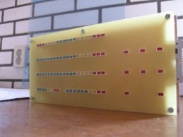
The LED board can be split in different sections. These sections are: Anode-Voltage meter, Forward-Output meter, Anode-Current meter, Grid-current meter, Reflected-Power meter, Fault-LED's and Periferal Supply. The periferal Supply is not physically located on the LED board, but finds his own place in the cabinet.
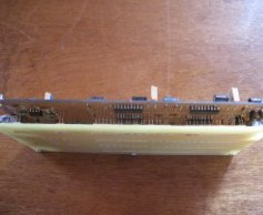
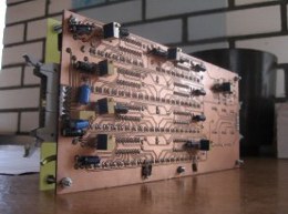
Once the schematics and the PCB design is finished, building the board can start. On this picture you can see the result of this work in the two pictures below. On the left the front site of a stackup, were the first panel is used for aligment of the LED bars only. Behind this piece of un-coppered PCB material (cheap...) is the board that holds all electronical components. On the back of this board are the adjustment controls. This allows adjustment for all the functions after building into the PSU housing.
   Front and rear panel:
Now it is time to start building the first components into the cabinet. I started on the front and rear panel. The front panel holds the LED bar PCB and no more than three buttons to control the PSU: ON/OFF, HV-ON and Reset. This reset button is connected to the controlboard that hold all the safety circuits. These safety circuits locks the PSU in case of errors. The seperate erros that blocks the PSU for operating are listed above. A simple press on the Reset button starts the PSU for operating again. A nice feature of the controlboard is the function that after pushing the Reset button, the large toroid transformer is re-connected again by using the soft-start. During safety-state the PTT is locked and cannot control any function in the PSU.
 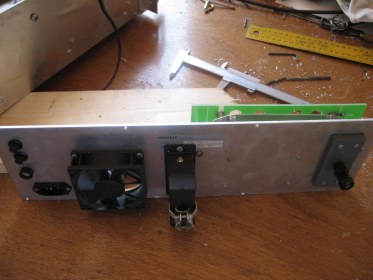 In the two above pictures are respectivily the front-, and rearpanel shown. The rearpanel hold three fuses, a small 12V blower that, in case of too warm transformer can be switched ON. Until today this blower is not been needed, even during extensive transmit periods during JT65b and using well over 1kW of RF output signal.
On the right of the rearpanel, the HV-feedtrough is located. This is a simple piece of PVC material of 10mm thickness. In the middle is a heavy-duty banana jack located. Behind the banana-jack is a large hole in the aluminum panel to prevent arcing. The connection for HV towards the cavity is made from a 1 meter long piece of RG213, of which the shield is connected to ground at the cavity side. After connecting the inner of this RG213 to the banana-jack, the assebly is covered with a small plastic box to prevent unwanted touching.
Filling the cabinet:
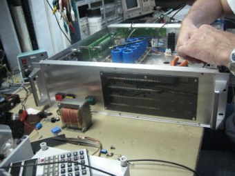
The interior of the cabinet is still empty...This needs change!
It is now time to install the capacitor bank, inrush resistors, safety resistors in series to the anode voltage output, periferal power supply for the LED board and the power darlington for the bias-circuit. After the mechanical work is done, it is time for the wiring and testing.
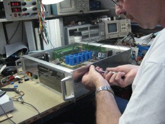  Completing the interior of the PSU is the last step in the building phase of the 144MHz power amplifier. Now tests can start to check on the functionallity and make adaptions to the design when needed. It turned out that minor changes were needed in the functionallity of the controlboard. The second unit (for 432MHz) turned out to work first time according plan.
Testing the assembly:
In the below shown picture is the combination PSU and cavity shown to work. The HV-supply shows a kind of orange stripe in the picture, this is due to SSB modulation during photography. This causes the anode-voltage to vary a bit, resulting in moving of the DOT-mode Bargraph display. All the other LED bars function in bar-mode and show fast reaction and slow decay. This helps to be able to determine maximum output power and anode-current during normal speech. That is also the reason why the analog Power-meter on top of the cavity show only 400W, were the PSU indicates a momentary peak in SSB modulation of around 800W.
 Now also the build-in directional coupler in the cavity output comes in. Because the here shown SWR/POWER meter is not capable of display 1kW+, the LED-bar in the PSU is not in danger of being burned out. After calibration is complete, the analog Power meter can be removed from the TX line towards the antenna. This also eliminates the need of using the RF banana-plugs at the rear of the comercial power-meters that can indicate upto 2kW in the VHF range. In my case I can connect the TX cable to the cavity by using 7/8" coax cable and using the correct connectors for this.
|