350W_JRC_Amplifier
(Powerwave NAH-2140D)
This chapter describes my experiences on the Powerwave NAH-2140D amplifiers as was sold a lot on the internet. The amplifier is designed to be used for amplification of digital signals in the 2GHz band. Remember: my experiences my differ to other users as there are different versions of the Powerwave amplifier. Other types uses different components and may run directly at 2320MHz...
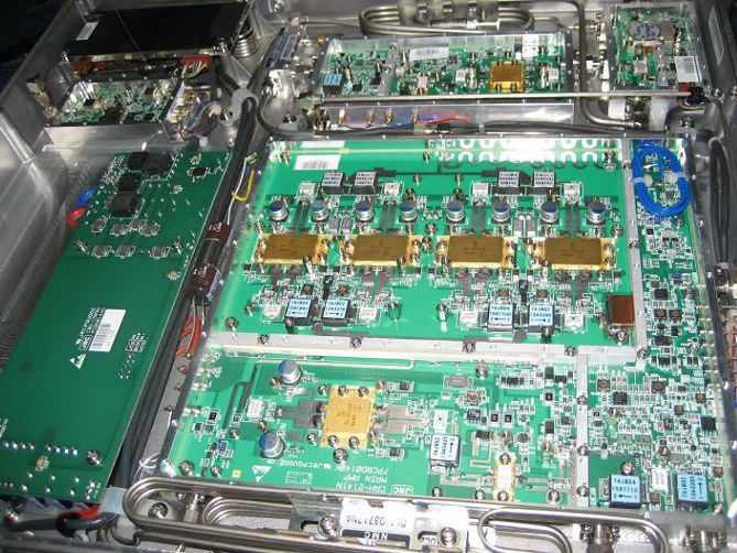
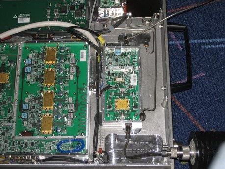
The amplifier was available in various variants, variating in output power from maximal 100W to 400W. I already owned a PCB from another type of amplifier (see other link to the left) and for this PCB I needed a backup in case it would be non-operational in the future. I ordered a second one in the original housing as a complete set, but the seller send me this unit. It does not have the 4 pieces MRF21085 in the final stage but instead 4 piece FLL1501IU-2C GaAS FET's from Fujitsu. In the below picture you can see the interior of this new received box:
First thing to do was to find out what the possibillities were with this unit. Few questions that come up are:
 Is this amplifier usable at 2320MHz without any changes? Is this amplifier usable at 2320MHz without any changes?What are the components that are inside the amplifier?
Are the power-FET's still OK?
What are the specifications of these power-FET's?
Initial tests on the total amplifier:
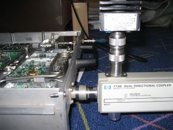
To answer the first question, the most important one, I connected the amplifier as I bought it to a spectrum-analyser with tracking function. To prevent damage to the input of the spectrum-analyser, I used a directional coupler and additional attenuators to bring the output of the amplifier down by -60dB. In case it would deliver 400W (!) the spectrum-analyser is not in danger.
In the picture here you can see the directional-coupler that is connected towards the input of the spectrum-analyser.
Because I did not wanted to risk the directional-coupler I later added a 10dB 350W attenuator in front of the directional-coupler. At the output of the directional-coupler is yet another 10dB attenuator to serve as load. In total the amplifier will see -40dB return loss (2 x 10dB attenuators in series).
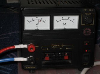
To test the amplifier, I first needed to study the supply-voltage. The original input supply-voltage of the amplifier is 48V@11A maximum. Inside the box is a converter that generates +12.5V for all GaAS-FET's as well as +5V and -5V. The -5V is very important because this is used for BIAS to the FET's. After some time spend I still could not get the +12.5V running. I decided to connect an external PSU (MANSON) that was set to +12.5V. The PSU can deliver 30A, enough for initial tests. If you do the same, aways remember first to switch the -5V and after that the +12.5V! If not set -5V the FET's draw a lot of drain-current because they are not biassed!
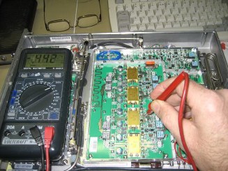
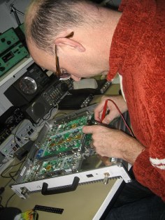
After checking again all connections, I first measured the functions of all BIAS-circuits. In the picture here you see me measure one of the negative voltages in the final-stage (-0.442V). All other FET's had approximately the same negative voltage. This was the moment to add the +12.5V to the FET's drain input.
In the picture here you can see the +12.5V power-supply that is switched ON after I checked the presence of the negative bias-voltages. The total amplifier draws about 10A idle...
Now the next step is to check the passband for the amplifier and see how the performance at 2320MHz would be. As said before I use a spectrum-analyser with tracking function to measure.
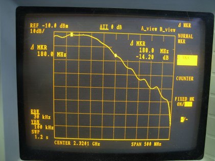
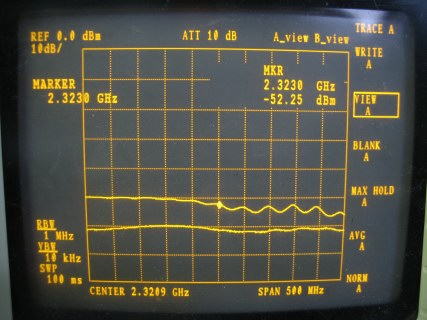
Saidly enough, the original unmodified amplifier is not usable for 2320MHz. The below picture shows this. The small-signal amplification (0dBm input) is already down by -14dB compared to the original operating frequency (2140MHz):
This picture is taken by using the delta-marker method. The left marker was set to 2140MHz, the right marker was set to 2320MHz.
Clearly visible the -4dB drop in gain measured in relation to 2140MHz. This was a dissapointment because now I had to find a way to overcome this situtiation.
Using the ERROR-AMP:
More study on the amplifier learned it consists of a MAIN-amplifier, an ERROR-amplifier, a SMPS (Switched Mode Power Supply), a Circulator-Unit and some other boards. The ERROR-amplifier uses a FLL601IU-2C GaAS-FET that is rated 60W output according its datasheet. After finding the total amplifier not suitable for 2320MHz, I studied the ERROR-amp more in detail: Is this unit OK at 2320MHz so at least this part is usable?
 The error-amplifier was tested seperate to check its usabillity at 2320MHz. I connected semi-rigid coax directly to its in-, and output and again used a spectrum-analyser with tracking function to observe the passband. This measurement showed also a significant drop at 2320MHz, leaving me more and more frustrated on the buy. It was told only the delaylines needed to be changed to use this version at 2320MHz, but more and more I come to the insight this might not be true at all... The error-amplifier was tested seperate to check its usabillity at 2320MHz. I connected semi-rigid coax directly to its in-, and output and again used a spectrum-analyser with tracking function to observe the passband. This measurement showed also a significant drop at 2320MHz, leaving me more and more frustrated on the buy. It was told only the delaylines needed to be changed to use this version at 2320MHz, but more and more I come to the insight this might not be true at all...
I started trying to modify the error-amp in such a way that at least this part was usable for 2320MHz. But were to start? I found that changing the seperate stages one by one was the best way to proceed.
Every stage is coupled to the next stage by coupling capacitors. I assumed that at these points the impedance is 50 Ohm so I could take the signal out for tests. I also discovered by measurements that the input was filtered. This was solved by using a piece of semi-rigid coax that now connects the input SMA-connector to the MXU35 FET.
Working my way forward, I could be proud at the end. Final result after adding copperfoil here and there and changing some capacitors, I achieved 40W RF output at 2320MHz. The error-amp now consumes at 12.5V about 11 ampere.
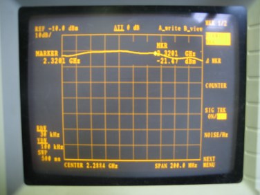
This picture shows the final results of all the tweaking that was needed to get the error-Amp working at 2320MHz.
The here shown picture clearly shows the passband is now almost exactly at 2320MHz. Center of the screen is 2320MHz, lowest frequency is 2220MHz and highest frequency is 2420MHZ (SPAN=200MHz).
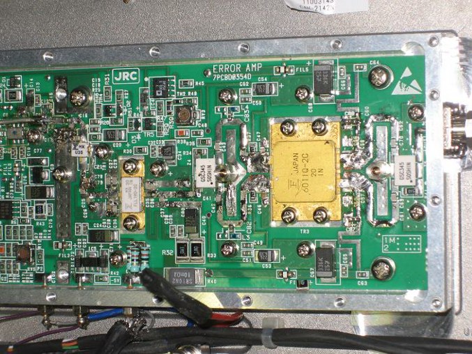
In the below picture you can see especially around the FLL601IU-2C GaAS FET the modifications I did. I have added copperfoil to the input of the Gate as well as copperfoil to the output near the Drains. The modifications around the two driver FET's (MXU35 and FLL190) are not so clear visible.
Work on the Main-amplifier:
After concluding the work on the error-Amp, I continued to work in the same way on the main-amplifier. I again used a small piece of semi-rigid to bypass the two filters at the input. The main-amplifier uses the same FET's as used in the error-Amp: MXU35, FLL190, FLL601IU-2C but in addition 4 parallel FLL1501IU-2C FET's.
I worked my way forward step by step by modifying stage by stage. Everytime I checked the improvements in the passband that was unacceptable dropping at 2320MHz. At some day I achieved 4W RF to drive the FLL601IU-2C that drives the final stage. I hoped this stage would give some 8-9dB that would be sufficient to get some 300W RF output.
However after long trying I did not succeed in getting the FLL601IU-2C stage to operate at 2320MHz. All effort was stopped and I wanted to tried to connect the already functional error-Amp to the input of the final stage of the Main-Amp. To be sure on the pasband of the final-stage I first connected semi-rigid coax to one of the input and output of the FLL1501IU-2C stages. Therefore I cut the PCB-traces that run to-, and from the Soshin baluns. This is needed to cut to have 50 Ohm points to connect.
After modifying the output, I achieved a gain in this stage of 9dB. This proves that the final stage of this powerwave amplifier can be used after small update. I must admitt that this only is valid for measuring only one of the four parallel stages, but it was looking good.
In the above pictures you see me working on the final stage as well as a picture os the passband of one of the four power-GaAS FET's. The lower line is reference, the upper line is the measurement. At 2320MHz there is 9dB gain after modifying the output-line were the two drains are connected to. I I needed to make them more wider.
Status 20-2-2010:
One of the soshin baluns at the input of the FLL1501IU-2C that I used to measure the above is damaged mechanically. To be able to do the measurements, I soldered a semi-rigid and after some movement, a piece of the ceramic material broke off. Now I am in doubt what to do; search a replacement or start a new design that is especially calculated for 2320MHz. Meanwhile I have the S-parameters for the FET's so I can calculate the needed impedances of the in-, and output lines.
|