TTE1482 experiments
This section descibes an experiment I started some years ago. I got my hands on 4 Motorola amplifers that have been in service for the old ATF2 mobile phone network. I wanted to combine these to a 800W solid-state amplifier. Each single amplifier was UHF broadband 200W output. After some time I decided to build a GS35b cavity that gave much little trouble in succeeding...
 What is a TTE1482e amplifier?
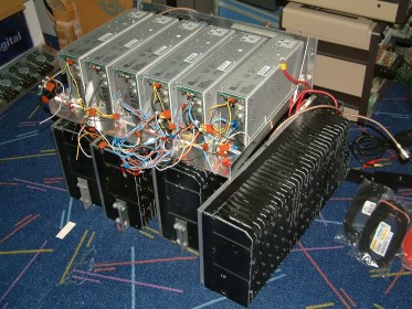
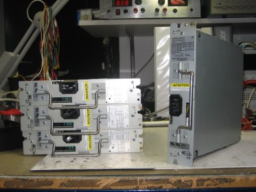
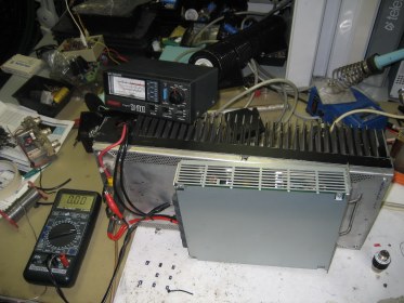
On the first picture in this part you see a pile of heatsinks and on top of this a few switched-mode powersupplies. The heatsinks are the coolers of the UHF broadband power-amplifiers, originally build by Motorola and named TTE1482e. One of this amplifiers is rated to deliver 200W continuous RF-power in a wide frequency range of 450 - 470MHz. They are originally set in class-C.
 The TTE1482e amplifiers consists of three succeeding stages equipped with a single transistor, followed by a final stage that holds a double transistor stage with two transistors in parallel. The supply-voltage is 12-15V, consuming at maximum output-power a DC current of 25-30A! The TTE1482e amplifiers consists of three succeeding stages equipped with a single transistor, followed by a final stage that holds a double transistor stage with two transistors in parallel. The supply-voltage is 12-15V, consuming at maximum output-power a DC current of 25-30A!To be able to use these amplifiers for 432MHz, the circulator-unit at the output of the amplifiers needs to be removed. This leaves an empty space as can be seen in the left shown picture.
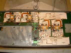
Inside this area is a new board is mounted that holds a
4-piece bias-unit. This bias-unit is necessary to bias the 4 transistors in this amplifier for class-AB1 mode (SSB).
Output connector:
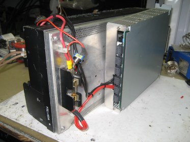
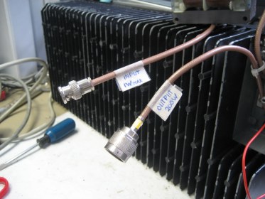
After removing the circulator-boards from the amplifier, also to coaxcables for the output are removed. That is why a new piece of coaxcable must be soldered to the spot were the original circulator input is removed. In this picture is showm how the teflon coax from the output of the circulator board is re-used and attached to the final-stage. Take a look at the strength-relieve were the outer conductor of the coax is soldered at two places to ground.
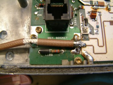 In the picture above is also the forward output coupler seen. This gives a DC voltage that is in relation to the momentary RF-output power. The DC-voltage is available at the modular-jack connecter, together with the DC-voltages that shows the current through each transistor-stage.
First tests:
The firsts tries on these amplifiers were performed at my QRL. There I have the access to nice measuring equipment like a Spectrum-Analyser and some nice directional couplers. Also a power-supply that is capable of delivering the needed 30A peak is available there, borowed from the Ericsson Radio Club PI4ERI.
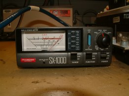 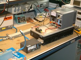 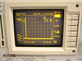 The tests on the workbench were very succesfull. The achieved output-power was for all four units nearly 200W, this is shown for one of the amplifiers on a Daimond SX1000 power/VSWR indicator. The use of a directional coupler at the output of the ampifier under test gave the possibility to measure also at the same time the harmonics. This is determined to be -35dB for the first harmonic. This is not enough to use the amplifier without any Low-Pass filter...Power output levels above 200W were not possible to achieve using the shown PSU in the above picture on the left side. At 30A the voltage dropped and this limited the maximal output power.
Coupling four units for QRO:
My goal was to use four of these units in a parallel stack for contest and EME. I was lucky to purchase 4 units from a duth HAM in one set, however there was no power-supply available that could deliver 12-15V/120A...
 This put me to the task to decide what to do; I have the access to another MANSON 30A Power-supply, but still two others were missing to feed the 4 units at the same time.
During some construction work at my QRL in the computer department, I traced some scrap material. Inside these racks were 5V/70A switched mode power supplies. A lot of current, little low in voltage however. Luckily I was able to trace 6 if these units, 5 at first instance, the 6th unit came from the computer department when cleaning the spare-spart out from the storage room. Advice: always keep your eyes and ears open for scrap materials!
Now I was able to connect 3 units of 5V/70A each in series, giving 15V/70A. This is sufficient to supply two ampifier units. The other 3 PSU'swere also connected in a series onfiguration, able to supply the other 2 amplifiers. All in all it already became an impressive pile of material, also because of the heavy weigth heatsinks on the amplifiers.
Improved PSU solution:
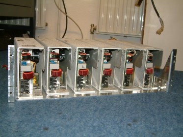
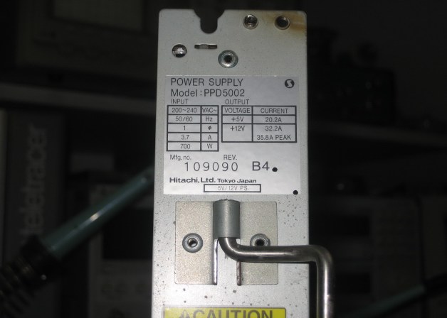
In February of 2007, I found some switched-mode power-supplies PPD5002 from Hitachi which, per unit, were capable of supplying sufficient power to one amplifier. I purchased 4 of these PSU's, having an adjustable output voltage of 12-14.7V DC, at peak currents of over 35A!
  To the left, the 4 new 700W switched-mode power-supplies that can substitute the 6 old 5V/70A power-supplies are shown.
The new power-supplies are much easier to use because a 1 single TTE1482 power-amplifier (200W out), also needs only a single power-supply is needed.
The new power-supplies needed one minor modification internally, a strap must be soldered as indicated on the casing. This normally is external when placing the PSU in a rack.
 Here the PSU is for the first test connected to the 70cm amplifier. I have doubled the wiring to the supply (2 x 6mm2) to have minimal losses in the DC lines because of the expected 30A. In the picture also the huge gold-plated fuse is seen. These fuses are often used in car hifi.
A small switch acts as PTT. When activated, the amplifier is set to idle current enabling SSB-operation.
 To run the TTE1482 in SSB, I needed to add four BIAS-circuits. These enable the four transistors to be set to class-A.
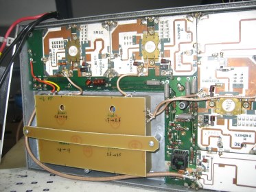
In the picture the BIAS-unit is shown, mounted in the space were the circulator-board is removed. The circulator was limiting the frequency range were the amplifiers could be used. After removing it, the amplifiers turned out to be usable from 430-470MHz.
The schematics for this BIAS units is derived from a combination of the original Motorola Application sheet and the drawings send from Ferdinand DC8EC and Alfons, DD5OI. These German HAM's made a description, see link: Link. With this description it is possible to turn the original class-C into class AB for SSB usage.
I personally did not like the used layout of this BIAS circuit and did my own, see this Link.
The PCBA in the link here must be build twice, this gives you 4 bias circuits for the 4 stages. The PCBA is double-sided, TOP-side is all copper, BOTTOM-side contains traces. GND connections for the components are all made at the TOP-side. The .sch and the .brd files are the EAGLE CADSOFT design files.
Use the original link to the .pdf made by Ferdinand DC8EC and Alfons, DD5OI to locate the 4 positions where to disconnect the component from GND marked as Ub-E. The disconnected pins are then RF-blocked to GND by a 1nF capacitor and at this point the bias-voltage from the new biasboard is inserted.
When adjusting the bias (PTT_input to GND), start with all 4 bias-circuits at 0V DC. Measure the DC current in the total supply (12V) and start with adjusting the bias_voltage for stage_1. Increase the total current from 0.1A to 0.9A (800mA current in stage_1).
Then increase the bias_voltage for stage_2 from 0.9A to 1.7A (also 800mA in stage_2). After this, increase the bias for the first output_stage from 1.7A to 2.6A (900mA in stage_3) and lastly increase the bias to the second output_stage for a total current from 2.6A to 3.5A (also 900mA in stage_4).
In case you want these re-drawn files, please contact me and I will help you further on this.
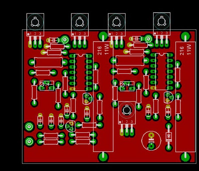
This new PCB is shown below to give an impression. This PCB hold 2 of the 4 needed BIAS circuits per Power-Amplifier. The TO-220 transistors are to be mounted on the heatsink (ELECTRICALLY ISOLATED, Thermaly conductive!) inside the TTE1482A PA. There is enough room available after removal of the circulator board. The PCB is double sided, top-side all copper, bottom-side holds all tracks. The two BIAS boards are mounted inside a screened box, in my case made from single sided PCB material. PTT_input, 12V_Supply and bias_out are connected by using 1nF feedthrough capacitors. The connections to the base of the four different power-transistors in the UHF-PA are made from screened cable.
   Using the new PSU's:
First tests indicated very stable output power. After enabling the BIAS-current (PTT to ground), the voltage to the amplifier dropped 300mV from the 14.7V that was set without load.
A tranceiver was connected to the input. A 10dB attenuator was inserted to the input of the amplifier. The tranceiver (TS811e) is standard capable of 25Wmax, with the 10dB attenuator as safe 2.5W to the input of the amplifier is maximum. The PA input power is now adjustable at the tranceiver between 300mW and 2.5W.
Power to the PA was slowly increased until the 200W output was reached. Looking at the input power, I was surpriced only to need 900mW for the 200W output. 1W at the input gave even a bit more output, but the 200W output should not be exceeded to far. Compared to the tests that were done earlier, it is indeed confirmed that the 200W maximum level found earlier was limited by the maximal 30A current of the PSU that was used at that time.
RF-Coupler:
To connect the amplifers for RF, I used at the input a ordinary 4-way splitter/combiner that is also found in antenna-systems. This is a square tube, in the middle and at both ends N-chassis parts. Each output gives a -6dB port, that is phase-equal to each other and is to be connected to the 4 inputs of the amplifiers.
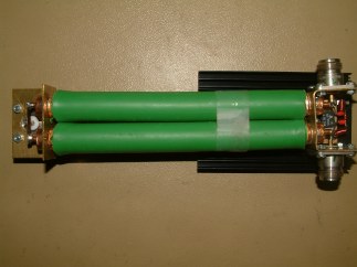 To connect the outputs is not a easy task. I tested first with two amplifiers on result. It turned out to be difficult to achive the same phase-shift in the two paths. The coupling device for the output was a device like shown in the picture on the left hand side.
It is constructed from two quarter-wave pieces of Coax-3 cable, at the combining port in parallel, at the two inputs bridged by a 100 Ohm, low-L resistor. These kind of couplers are known as Wilkinson-divider.
Across the 100 Ohm resistor is a RF-detector mounted to be able to measure any difference in power at the two ports. The detected RF-voltage is avaible on a feedthrough capacitor in the heatsink of the resistor.
The two seperated inputs ports (left upper and lower N-chassis part in the picture) are transformed to 100 Ohm each at the combining port (left side N-chassis part in the above picture). The two ports are in parallel connected, giving 100/2 = 50 Ohms.
I was able to achieve 360 Watt RF-power on two amplifiers. The inputs of the amplifiers were not connected directly to the input-coupler. Instead of this, variable attenuators and in one leg a phase-shifter was placed. With this setup, I was able to compensate the difference in the two amplifiers for gain, output power and phase-shift.
To my believe this phase-differences in the two amplifiers under test were introduced by the three transistor-stages in series. This will introduce errors. Also I measured that the phase per amplifier changed at different RF-levels at the output. Pfffff......
Project discontinued:
I decided not to continue on the combination of four amplifiers. I changed over to the build of a GS35b tube amplifier for 432MHz, that is now in full service for quite some time without much problems. This project is described here: link to the left.
In future I think of running the 4 amplifiers (200W SSB each) to seperate, fixed direction antenna's during a contest. Together with the rotating main antenna-system, this will result in a total setup that is less sensitive to the main beam direction. During a contest, it is important that all directions should be supplied with signal. This rises the change of succesfull QSO's.
|